
A semiconductor fabrication facility, or fab, turns polished silicon wafers into hundreds or thousands of identical integrated-circuit dies by repeating a tightly controlled patterning cycle. The cycle deposits films, coats photoresist, projects circuit patterns with lithography, develops and etches the surface, implants dopants, cleans the wafer, and measures the result. A modern chip may require as many as 100 aligned layers, and the complete path from design release to volume production can take up to four months.
The key idea is that a chip is not printed in one pass. Each wafer carries many copies of a design, and every layer must line up with the layers below it at nanometer scale. Cleanroom control, inspection and yield engineering determine how many of those copies become usable products.
As an Amazon Associate I earn from qualifying purchases.
What a semiconductor fab actually does
A fab is the front-end manufacturing plant where transistors and the wiring that connects them are built on silicon. It is one part of a larger value chain: companies create circuit designs, a fab fabricates the wafer, and a back-end operation cuts, packages and tests the finished dies.
Recommended Free Tools
Wafers move through hundreds of named operations and, in some factories, thousands of individual tool steps over several weeks. Including process qualification and the transition from an approved design to volume production, the journey can extend to about four months. The duration is not a single uninterrupted machine run; wafers repeatedly leave one tool, undergo measurement or cleaning, and return for another operation.
#1 Best Overall

- BLUE LIGHT BLOCKING GLASSES: Our blue light glasses for women boast UV400 protection, blocking harmful blue rays from computer screens. With these bluelight glasses women, you can enjoy gaming, reading, or watching TV with no worries of eye strain.
- EYE RELIEF: Our blue light glasses are engineered to reduce blurry vision or strain caused by prolonged screen time. These womens blue light glasses aid in better sleep by preventing blue light from disrupting your natural sleep cycle, helping you fall asleep faster and enjoy a more restful night's sleep, making them the perfect christmas present.
- COMFORTABLE: Crafted from durable material, our trendy blue light glasses for woman or blue light glasses men ensure long-lasting comfort. The high-transmittance lenses accessories, gamer gifts for men, help keep your eyes relaxed. Perfect stocking stuffers, gifts for gamers men, christmas gifts for men, halloween costumes.
- LIGHTWEIGHT: These clear blue light glasses feature a lightweight frame, meaning they’ll stay comfy for long-term wear. Perfect as blue blockers glasses for women or mens blue light glasses, these non-prescription fake glasses for men can be worn throughout the day. The blue light blocking glasses women feature polycarbonate HD lenses, which are anti-reflective and restore true color.
- WORRY-FREE PURCHASE: If you experience any issues, our support team is ready to assist you quickly. These are the perfect costume glasses for cosplay dressing up.
For a game console, graphics processor, CPU or memory device, the same principle applies: a large circular wafer is processed as a batch, producing many small rectangular dies in parallel. Parallel processing is what makes high-volume chips economically practical.
Front end versus back end
- Front-end wafer fabrication: Builds transistor structures, isolation regions and multiple levels of metal interconnect on the wafer.
- Back-end assembly and test: Separates the dies, attaches each one to a package, makes electrical connections, adds protection and heat-spreading features, and verifies operation.
The package is part of the product’s electrical and thermal design. It controls how signals leave the die, how power is delivered and how heat reaches a cooler; it is not merely a protective box.
From refined silicon to a usable wafer
Manufacturing starts with silicon refined to electronic-grade purity and grown into a single-crystal ingot. A diamond saw slices the ingot into thin discs. Grinding and chemical-mechanical polishing create an exceptionally flat, smooth surface suitable for nanometer-scale patterning. The polished disc is the shared substrate on which many copies of one chip design are fabricated.
PC Slower Than It Used to Be?
A free scan shows the junk files, broken settings and background clutter dragging Windows down - then fixes them in one click.Free scan · Windows 10 & 11Outdated Drivers Are Slowing You Down
One free scan finds every outdated or missing driver and matches the right update for your exact hardware.Free scan · exact hardware matchCommon wafer diameters
| Diameter | Informal name | Where it fits |
|---|---|---|
| 300 mm | 12-inch | Large-volume production; more die sites per wafer when the process and equipment support it |
| 200 mm | 8-inch | Widely used for established processes and specialized products |
| 150 mm | 6-inch | Still used for some mature or specialty manufacturing |
Diameter alone does not predict cost or output. A larger wafer offers more area, but the useful number of dies also depends on die size, edge exclusion, defect density, process maturity and how efficiently the factory can run that wafer format.
The repeating fabrication loop
Each layer follows a related sequence. The exact chemistry, temperatures, film thicknesses and measurement points vary by process, but the purpose of each stage remains recognizable.
1. Deposit a film
Tools add a thin layer of conducting, insulating or semiconducting material. Deposition may cover the entire wafer, after which later patterning removes selected regions. Film uniformity matters because a thickness error can affect every die and every subsequent layer.
2. Coat the wafer with photoresist
A liquid, light-sensitive polymer is dispensed while the wafer spins. Centrifugal force spreads the resist into a controlled film. The coating must be uniform enough that exposure and development behave consistently from the center of the wafer to its edge.
Rank #2

- WINDEX GAMING WIPES: effortlessly clean all your gaming gear and gaming electronics in one easy step with our new Windex Gaming Wipes
- AMMONIA FREE: our ammonia-free formula is safe to use on all of your favorite gaming equipment like consoles, headsets, controllers, screens, keyboards, and more
- PRE-MOISTENED WIPES: each wipe instantly removes dust, dirt, and stubborn smudges and fingerprints leaving a streak-free shine
- ANTI-STATIC: great for cleaning and wiping down your gaming gear and electronics leaving behind no visible residue
- COMPACT RESEALABLE PACKAGE: store your pack of Windex Gaming Wipes anywhere in your home for whenever a quick and easy wipedown is needed
3. Expose the pattern with lithography
A reticle carries one layer of the circuit blueprint. The lithography tool illuminates that pattern and uses precision optics to reduce and focus it onto the resist. Some systems transmit light through the reticle; others reflect it. The exposed resist undergoes a chemical change that allows the next development step to distinguish patterned and unpatterned regions.
4. Bake and develop
Thermal bakes stabilize the resist and complete the intended chemical reactions. A developer solution then dissolves either the exposed or unexposed portions, depending on the resist formulation. The result is a temporary stencil: openings reveal areas that will be etched, implanted or otherwise processed.
5. Etch the exposed material
Dry etch uses a plasma of reactive gases to remove material with directional control, while wet etch uses liquid chemistry. Engineers select a method according to the film, the required profile and the risk of damaging neighboring features. Etching converts a flat deposited film into three-dimensional lines, holes, trenches or isolation structures.
6. Implant dopant ions
An ion-implantation tool accelerates charged atoms into selected regions of silicon. Dopants change the local electrical behavior of the crystal, allowing engineers to form transistor source and drain regions, tune threshold voltage and create other active structures. A later heat treatment repairs crystal damage and activates the dopants.
7. Strip the resist and clean
After its pattern has served its purpose, the remaining resist is removed. Plasma ashing, wet chemicals and rinsing clear residues and particles. Cleaning is repeated throughout the flow because a contaminant left on the wafer can spoil an otherwise correct layer.
8. Measure and inspect
Metrology tools measure critical dimensions, film thickness, overlay, electrical properties and surface profiles. Optical inspection finds many defects quickly; electron-beam methods can examine smaller features or classify a suspicious site in greater detail. The measurements feed statistical process control, which can adjust recipes or tool settings before a drift affects more wafers.
What lithography means in plain language
Lithography is best understood as a projection system. The reticle pattern is larger than the feature ultimately printed. Optics shrink the image and focus it onto photoresist, and the developed resist then protects selected regions during etch or deposition.
Rank #3

- Ergonomic & Adjustable Design: Fight "text neck" and improve your posture. Designed for comfort, it offers an adjustable height (7.1in-8.5in) (1.4in adjustable range) and angle (5°-85°) Please note: cell phone stand is only 9 inches tall—the length of a standard pencil
- Without blocking subtitles Perfect for office desk Tiktok Face Time Zoom video—this is the ultimate kitchen desk essential for phones! Perfect viewing experience while reducing neck back strain, A must-have for gamers streamers desk, and anyone who values both style and support!
- Sleek & Stable Design fits Otterbox Case: Say goodbye to bent cables, tangles, and tip-overs! LISEN’s stylish adjustable desk phone holder features a built-in charging hole and smart cable management, keeping your phone secure and your workspace clutter-free cool gadgets for men
- ANTI-SLIP DESIGN free hands: The under 10.00 items easy gadgets back and the bottom of this kitchen essentials for women are fully covered by anti-skid silicone, which LISEN stand up desk decor can provide maximum protection device from any scratches and slides
- Your Perfect Viewing Companion:If your product arrives damaged or breaks within 365 days, reach out to LISEN for a quick and hassle-free solution. Struggling with assembly, like tightening the screw? We’ve got your back! Your experience matters to us. (Product including: phone Holder stand*1, screw*1, hexagon screwdriver*1, specification*1)
EUV and DUV roles
Extreme ultraviolet (EUV) systems are used for the smallest critical layers in advanced processes. Deep ultraviolet (DUV) systems handle larger features and many layers that do not require the shortest wavelength. A modern fab commonly uses both; EUV does not replace every other lithography step.
What’s actually slowing this PC down?
Pick the symptom - the matching free tool is one click away.
Alignment across layers
Every exposure must register with marks created in earlier layers. Overlay error means the new pattern is shifted relative to the old one. Because a chip can contain up to 100 layers, a small systematic error can propagate through many dies. Alignment measurements are therefore taken repeatedly, and the scanner applies corrections as the wafer moves from field to field.
Computational lithography
At very small dimensions, diffraction, resist chemistry and lens imperfections distort the pattern that would result from a literal image. Computational lithography uses models, tool data and test-wafer measurements to pre-correct the reticle pattern or exposure conditions. The goal is not just a prettier image; it is a pattern that prints reliably across process variation, improving manufacturability and yield.
Why a fab must be extraordinarily clean and stable
A particle large enough to see can destroy a die feature that is only a tiny fraction of its diameter. Fabs therefore filter and recirculate air, move wafers in sealed carriers and control personnel movement. Cleanrooms described as ISO Class 1 can be about 10,000 times cleaner than ordinary outside air.
Particle control is only one part of stability. Temperature and humidity affect resist coating and chemical reactions; vibration can blur a lithography exposure; trace metals can change device behavior; and tool calibration determines whether a recipe remains inside its process window. Facilities monitor chemical purity, airflow, pressure, vibration and equipment health continuously.
The Tool Desk
Outbyte PC Repair FREEClear out junk files and repair common Windows errorsFree Scan →Outbyte Driver Updater FREEScan for outdated or missing drivers - takes under a minuteDriver Scan →Why control is economical, not cosmetic
A defect introduced early can be repeated in every later layer and across every die on a wafer. Preventing one contamination event may save an entire wafer lot. This is why fabs invest in automated material handling, redundant filtration, frequent calibration and statistical alarms rather than relying on a final inspection alone.
Yield: the number that connects physics to business
Yield is the percentage of usable dies produced from a processed wafer. A wafer can complete every scheduled operation and still contain a mixture of good and bad dies. The good dies are separated and sold or assembled; the bad ones are rejected.
Rank #4

- Easy Installation: Our gaming lights have been designed to enhance your entertainment experience. Simply position the led light bar next to your TV or game console to create a game room environment with ease. They come with USB power and a 60 inch cord for direct mounting and mobility
- Audio Syncing & Extensive Mode: The built-in high-sensitivity music sensor allows you to sync the TV led lights to your favorite music. Lights react and move to the beat of music, film and game audio, creating an incredible immersive sound and light experience – and all without the need for an additional hub. You can choose from 64+ patterns, including strobe, illusion, jump, energy, gradient, running, chasing, fluttering mode etc. Each mode can be applied to different scenes
- 64+ Chasing IC+RGB & W Effect: The independent control design of IC+RGB and white all-in-one multifunctional rgbw led bar lights monitor backlight allows you to easily switch the led lights for desk between IC+RGB and white to enjoy a variety of lighting effects, you can choose white lighting mode with high brightness for better illumination when working, etc. Choose IC+RGB lighting mode when you need to create an entertaining atmosphere for the light show, 16 million colours of Color changing rgb light bar let you dance to the beat and create a dynamic party atmosphere
- Dynamic and Dimmable Lights: 1%-full brightness free brightness adjustment gives you the flexibility to adjust dimmable led light bar for room decorations or a variety of occasions
- USB Powered: USB light bars for room can be powered by powernank, usb charger, TV, Monitor, laptop PC mainframe, making behind TV led lighting bar easy to install in any location.TV led lights are powered by the TV usb interface / PC mainframe, can be turned on/off synchronously with TV / PC
What lowers yield
- Particles, scratches or chemical contamination on the wafer.
- Non-uniform deposited films or unstable etch rates.
- Misaligned layers and excessive line-edge roughness.
- Defects in the reticle, resist coating or exposure field.
- Electrical failures caused by incorrect dopant concentration or thermal history.
- Process drift that moves a dimension outside its allowed range.
Defect density is especially important for large dies: a larger area gives each die more opportunities to intersect a defect. Process maturity generally improves yield as engineers learn the stable operating window, but no universal yield percentage applies to every product or factory.
How fabs improve yield
- Locate the defect: Inspection and electrical test identify where failures occur and whether they cluster by wafer, field, tool or time.
- Classify the cause: Engineers compare defect signatures with metrology, maintenance records and process conditions.
- Correct the recipe or equipment: Parameters such as exposure dose, focus, gas flow, temperature or cleaning frequency are adjusted within validated limits.
- Verify the change: Additional monitor wafers and statistical checks confirm that the fix reduces defects without creating a new failure mode.
Yield also affects capacity planning. If a wafer contains 1,000 potential die sites but only 850 pass all tests, the factory has produced 850 usable dies, not 1,000 saleable chips. That distinction influences cost, inventory and the number of wafers required for a product launch.
From finished wafer to packaged chip
Wafer sort and dicing
Electrical probes test dies while they are still connected to the wafer. A diamond saw or laser then separates the wafer along scribe streets, producing individual dies. Failed dies are discarded or retained for analysis.
Die attach and interconnection
A good die is attached to a package substrate or lead frame. Fine wires, bumps or other interconnect structures connect the die’s pads to the package’s external contacts. The choice affects signal speed, power delivery and mechanical reliability.
Protection and heat removal
Molding compounds, lids, underfill and other structures protect the silicon from moisture and mechanical stress. Heat spreaders or integrated lids provide a path to a cooler. High-performance processors may use advanced substrates or multiple dies in one package when the electrical and thermal design calls for it.
Final test
Packaged parts undergo electrical, functional, speed, leakage and reliability tests. Test results sort devices into product grades and catch assembly defects that wafer probing could not reveal.
Quick wins for a faster PC:
Fix the driver behind crashes, sound loss and screen glitchesFind Drivers →Clear out junk files and repair common Windows errorsFree Scan →Who operates a fab?
The word fab describes the physical plant. The word foundry describes a contracting relationship, so the two are not interchangeable.
Best Value
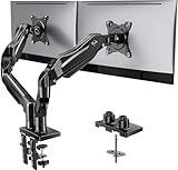
- Compatible with Wide Screens - To ensure compatibility with the dual monitor mount, your each monitor must meet three conditions at the same time: First, computer screens size range: 13 to 32 inches. Second, screen weight range: 4.4 to 19.8 lbs. Third, the back of the monitor screen must have VESA mounting holes with a pitch of 75x75mm or 100x100mm.
- Regarding the compatibility with desks - Your desk must meet three conditions at the same time: First, desk material: Only wooden desks are recommended, plastic or glass desks cannot be used. Second, desk thickness range: 0.59" - 3.54". Third, the bottom of the desk should not have any cross beams or panels, as this will interfere with installation. We recommend carefully checking that your desk and monitors meets all above conditions before purchasing.
- Dual C-Clamp Hold - Worried your dual monitors might wobble or slip? Our upgraded base uses a larger platform plus a dual C-clamp structure to lock the dual monitor arm firmly to your desk. Each arm safely keeps your screens steady while you type, click and game—no shaking, no sliding, just a clean and secure setup you can trust every day. It also provides Grommet Mounting installation choice, both options ensure stable and secure fixation for your 0.59" - 3.54" desk.
- Full-Motion Adjustment For Comfortable View - Pull the screen closer when you’re deep in a spreadsheet, push it back to watch videos, or rotate to portrait for coding — moving everything smoothly with just one hand. The monitor stand offers +85°/-50° tilt, ±90° swivel and 360° rotation. Raise your monitor up to 15.75″ to support a healthy sitting posture. Whether you’re working from home, gaming through the night, or switching between video calls and documents, getting the screens to your natural line of sight helps relieve neck, shoulder and back strain so you can stay focused longer with less fatigue.
- Keep Your Desk Organized: By lifting both screens off the desktop, this dual monitor stand opens up valuable space for your keyboard, notebook, docking station or a simple, clutter-free work area. Built-in cable management guides wires along the arms, keeping cords out of sight and out of the way. Enjoy a tidy, modern workstation that looks as good as it feels to use.
Integrated device manufacturer (IDM)
An IDM designs chips and operates manufacturing capacity for its own product lines. It controls the design-to-process feedback loop but must fund and fill its factories with internal demand.
Pure-play foundry
A pure-play foundry manufactures designs supplied by customer companies. It offers defined process technologies, design rules and capacity commitments while keeping customer designs separate. Its economics depend on serving many customers efficiently.
Fabless company
A fabless designer concentrates on architecture, verification and software support, then contracts wafer production and packaging to manufacturing partners. This model avoids the capital cost of owning a wafer fab but makes the designer dependent on external capacity, process schedules and yield.
Free tools Windows power users keep installed
One-click scans. No signup required.
How to compare two fabs or process technologies
| Comparison axis | What to ask | Why it matters |
|---|---|---|
| Feature size and node | What dimensions are controlled, and what does the process recipe include? | A node name is a process-generation label, not necessarily a literal transistor measurement. |
| Layer criticality | Which layers require the tightest dimensions and overlay? | Critical layers drive lithography, metrology and defect-control requirements. |
| EUV/DUV capability | Which exposure systems are available for the product’s layers? | Exposure capability limits what patterns can be printed economically. |
| Wafer diameter | Does the line run 300 mm, 200 mm or 150 mm wafers? | Diameter changes die count per wafer and equipment economics, but not yield by itself. |
| Process maturity | How long has the recipe run in volume, and how stable is its process window? | Mature processes often offer predictable yield for products that do not need the newest dimensions. |
| Defect density and yield | How many dies pass, and under what product and factory conditions? | These figures determine usable output; they cannot be treated as universal percentages. |
| Throughput | How many wafers can tools process per hour at the required accuracy? | Throughput determines practical capacity and delivery time. |
| Packaging | What substrate, interconnect and thermal options are available? | Package limits can affect bandwidth, power and cooling as much as the wafer process. |
| Business model | Is the plant an IDM operation or a customer-serving foundry? | The model affects design access, scheduling, ownership and supply commitments. |
A realistic timeline from design to mass production
- Design and verification: Engineers define the circuit, simulate it and check that it obeys the chosen process rules.
- Mask and reticle preparation: Each layer’s pattern is converted into manufacturing data and reticle structures.
- Process qualification: Test wafers establish deposition, exposure, etch, implant, clean and measurement recipes.
- Wafer processing: Production wafers repeat the patterning loop across all required layers, often over several weeks.
- Electrical sort and failure analysis: Dies are tested, defects are classified and yield trends are reviewed.
- Assembly and package qualification: Good dies are packaged and tested under electrical, thermal and reliability conditions.
- Ramp to volume: The factory increases output only as process capability, equipment uptime and yield support predictable shipments.
The often-quoted period of up to four months covers the broader transition from an approved design to mass production; an individual wafer’s time in the factory is a different, shorter measure.
Common misconceptions
- A chip is not printed once. Patterning, deposition, etch, implant and cleaning recur for every layer.
- Smaller node labels are not direct ruler measurements. They identify a coordinated recipe and generation of manufacturing technology.
- Every fab is not a leading-edge logic fab. Many specialize in mature-node analog, power, sensors, automotive devices or memory.
- A bigger wafer does not guarantee lower cost. Die size, defects, yield, equipment utilization and packaging determine useful economics.
- EUV is not used for every layer. DUV and other patterning methods remain important for larger or less-critical features.
- Yield is not a single factory score. It varies with product design, die area, process maturity and operating conditions.
- The package is not an afterthought. Electrical connections, power delivery and heat removal are designed together with the die.
Why this matters to game hardware
Modern game systems combine large logic dies, memory and high-speed packages. The fab determines how densely transistors can be arranged and how consistently each die meets its electrical targets. Yield determines how many usable processors or graphics dies come from each wafer, while packaging determines how quickly signals and power can move between the die, memory and the system board.
When a process is new or a die is unusually large, defects can reduce the number of sellable parts even if the design itself is correct. A mature process may offer lower density but steadier output for controllers, connectivity chips, power-management devices or other components that do not need the smallest features. Understanding that trade-off explains why one game device can use chips made on several different process generations.
How large the industry is
As a historical scale indicator, an industry manufacturing overview reported 1.15 trillion semiconductor units shipped worldwide in 2021—about 145 chips per person. That figure counts units across many categories, not just processors, and it illustrates why wafer-level automation, defect control and parallel production are essential.
Quick Recap
Product prices and availability are accurate as of the date/time indicated and are subject to change. Any price and availability information displayed on Amazon at the time of purchase will apply.

